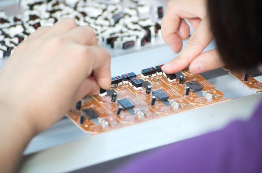
A solder mask is a shield to prevent molten lead from sticking to untargeted metals during solder operations. In printed circuit board solder operations, the goal is to form a conductive path between the conductive pad and the component lead. The solder mask ensures that there are no unintended short circuits created in the process.
Printed circuit boards hold the conduct traces and the electronic components in place. The blank printed circuit board is a thin sheet stuck to an insulator board, such as fiberglass or epoxy resin. A printed circuit board is processed first by using an acid mask to define the traces or electrical conductors that will remain when the board is immersed in a copper-dissolving acid, such as ferric chloride, in a process called etching. After etching, the board is cleaned and then printed with both labels and a solder mask or solder resist to expose only the connection points.

Chemical reactions are therefore important for the printed circuit board manufacturing process. A single-sided printed circuit board is first applied with an etching mask that exposes copper laminates that are to be removed. By the action of an acid, the masked portions remain.
After mounting the components on a printed circuit board, it is preheated and ready for soldering. The connections on the underside of the board may undergo a process called wave soldering, where molten lead comes in contact with exposed connection pads that are usually metal-plated copper. If a solder mask was not applied, the long runs of individual traces will get short circuited in the soldering process.
Mass production in electronics manufacturing makes use of solder mask film for preparing boards for soldering. A liquid solder mask is useful for printing the mask using silkscreen or other printing methods. Epoxy-type solder masks may be more resistant than lacquer-type solder masks.
An etched board will look like an insulator sheet with lines, which are patterns of copper conductors. The next step may be solder mask printing. The board can then be drilled to fit any components that need through-holes. For single-sided printed circuit boards, the only choice is to use through-hole components.
Once the components are mounted, the extra leads at the trace side will be cut. The next step is usually wave soldering, which will preheat the board and allow a wave of molten lead to progress through the underside of the printed circuit board. In the process the board is totally soldered in a few seconds, even with hundreds of solder points.
