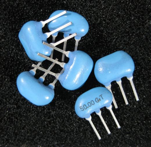
Semiconductors are an ever-present element in modern technology. When judged by their ability to conduct electricity, these devices fall between full conductors and insulators. They are used as part of a digital circuit in computers, radios, telephones, and other equipment.
The semiconductor manufacturing process begins with the base material. Semiconductors can be made from one of a dozen such materials including germanium, galium arsenide, and several indium compounds such as indium antimonide and indium phosphide. The most popular base material is silicon because of its low production cost, simple processing, and temperature range.

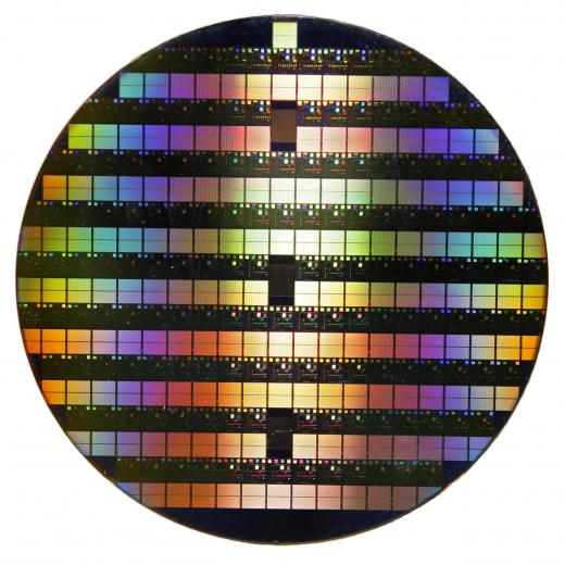
Using silicon as an example, the semiconductor manufacturing process begins with the production of silicon wafers. First, the silicon is sliced into round wafers using a diamond-tipped saw. These wafers are then sorted by thickness and checked for damage. One side of the wafer is then etched in a chemical and polished mirror-smooth in order to remove all impurities and damage. Chips are built on the smooth side.

A layer of silicon dioxide glass is applied to the polished side of the silicon wafer. This layer does not conduct electricity, but helps to prepare the material for photolithography. The manufacturing process also applies layers of circuit patterns to the wafer after it has been coated in a layer of photoresist, a light-sensitive chemical. Light is then shone through a reticle and a lens-mask so that the desired circuit pattern is imprinted onto the wafer.

The photoresist patterning is washed away using a number of organic solvents mixed together in a process called ashing. The process results in a wafer that is three-dimensional (3D). The wafer is then washed using wet chemicals and acids in order to eliminate any contaminants and residues. Multiple layers can be added by repeating the whole photolithography process.
Once the layers have been added, areas of the silicon wafer are exposed to chemicals in order to make them less conductive. This is done using doping atoms to displace silicon atoms in the original wafer’s structure. It is difficult to control how many doping atoms are implanted into any one area.
The final task in the semiconductor manufacturing process is the coating of the entire wafer’s surface in a thin layer of conducting metal. Copper is usually used. The metal layer is then polished to remove unwanted chemicals. Once the semiconductor manufacturing process is finished, finished semiconductors are tested thoroughly.
