Automatic test equipment performs complex tests on printed circuit boards, integrated circuits and other electronic devices. The testing usually takes place in a production environment where automated, relatively high-speed testing is important. Automatic testing equipment can use a variety of techniques, including functional circuit testing, optical examination and X-ray inspection. It is frequently used by semiconductor manufacturers to test microprocessors, memory chips and analog integrated circuits. Automated test equipment is also used by electronics manufacturers to verify the correct operation of circuit boards, avionics systems and electronic components.
An automatic test equipment device can be quite simple, performing just a few voltage and current measurements on the part being tested. Other systems are very complex, performing dozens of functional and parametric tests with a variety of test instruments. Some can vary the physical environment of the part being tested as well. For example, a device may be tested inside a chamber that is subjected to extreme heat or cold under computer control. Depending on the nature of the device, testing may also involve exposure to a range of light, sound or pressure.

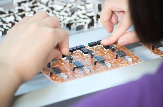
Assembled printed circuit boards with their parts already soldered in can be tested with a variety of automatic test equipment. Some systems employ optical inspection units which scan each board for solder problems including bridges, shorts and poor quality joints. These systems utilize high-resolution mobile cameras and are usually able to detect incorrectly placed and missing components as well. Test systems may also use three-dimensional X-ray inspection to discover problems which are not visible with standard optical inspection. For example, X-ray systems can "see" inside the solder joints underneath Ball Grid Array integrated circuits and flip chips.

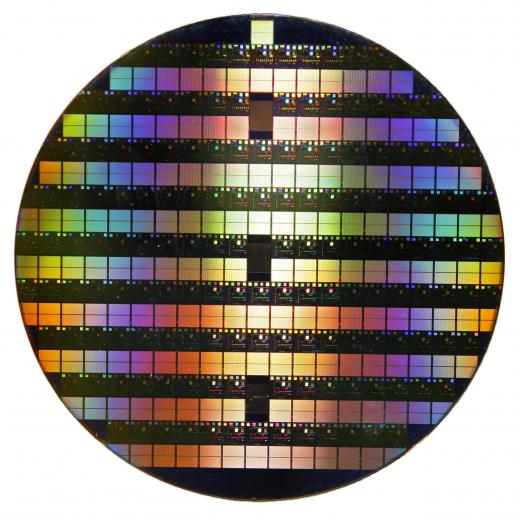
Many types of automatic test equipment include robotic handler systems which obtain and correctly position each part being tested. Depending on the type of device under test, a handler may rotate or re-position each device several times before all testing is complete. Silicon wafers in particular contain many individual semiconductor devices to be tested. The test equipment moves a robotic unit called a prober along the wafer from device to device during testing. It may also rotate or re-align the wafer if needed.
Once a physical device, circuit board or wafer has been completely tested, a robotic sorter can move it from the test station to one of several bins. Usually there are multiple bins so that problematic devices can be sorted according to which tests they failed. Some automatic test equipment environments include different test equipment at each of several stations. Devices under test may be moved from station to station by human workers or robotic handlers as appropriate.
